The original idea to this apparatus comes from an (now) old german crafts book for boys
"Werkbuch für Jungen" by Rudolf Wollmann. It uses car ignition coils as high-voltage
transformers and can produce several 10s of kilovolts in output voltage.
So don't miss this warning!!!
![]() The voltages and currents in the equipment described on this page
might be lethal or at least unpleasant if it is used improperly. I cannot be held responsible for any damage
that occurs due to information available on these pages.
The voltages and currents in the equipment described on this page
might be lethal or at least unpleasant if it is used improperly. I cannot be held responsible for any damage
that occurs due to information available on these pages.
![]() Be sure to take all necessary precaution when operating similar equipment and keep a safe distance
to the high voltage parts.
Be sure to take all necessary precaution when operating similar equipment and keep a safe distance
to the high voltage parts.
![]() When operating high-volatage equipment with open discharges, large quantities of ozone can be
produced. Make sure to have sufficient air flow.
When operating high-volatage equipment with open discharges, large quantities of ozone can be
produced. Make sure to have sufficient air flow.
1. History
2. Function
3. Construction
4. Operating
5. Pictures
The spark inductor was one of the first inductively coupled high voltage generator, used by
scientists, engineers and inventors from the late 19th century. The first reported spark
inductor dates back to 1851 and the german craftsman Heinrich Daniel Rühmkorff.
It where these kind of machines which powered the first gas discharge tubes by Lenard,
Geissler and Crooke, the first cathode ray tubes by Braun,
the first X-ray generators by Wilhelm Conrad Röntgen and the first
radio transmitters by Heinrich Hertz and Guglielmo Marconi.
Their principle is still found
today in a lot of voltage converters, like the high-voltage generation in computer monitors or TV sets,
and in the ignition circuit of a car engine. You might once in a while happen to see
one of these old hand-made inductors with polished brass gadgets in a museum or a school's
collection - they are pieces of art!
Some 15 years ago, me and my best friend found the corresponding chapter in the german book
"Werkbuch für Jungen" by Rudolf Wollmann. We decided to
build a set of two spark inductors from each two used car ignition coils and a mechanical relay as
interruptor. These were working fine, but it was impossible to run them for a longer time as
they consumed more power than our modell railroad trnsformators were able to deliver and
they surely were major sources of radio interference. Later I reconstructed the low voltage
side with a power bipolar transistor and some oscillator circuitry, but it didn't really work out.
Later my machine became a victim of my parents' cleaning-up-and-throw-away action. I don't know what
happened to it's twin, but I'm quite sure it doesn't exist anylonger either.
During the mid 1990s, I rebuild the machine from my memory, this time I applied my new knowledge
in electronics and constructed a fast switching low voltage side with a power MOSFET and a
kind of PWM circuitry using two monoflops. The performance was much superior to the old version,
but strangely enough so was this machine lost somewhere during my move from Germany to Sweden.
So it was time again - in the year 2000 - to build the model number 3. This time I actually
bought two brand new ignition coils - they are not so expensive and look much nicer - and decided
to put everything on the web. After some trouble I finally managed to get the thing going on
05-May-2000...
The principle function of the spark inductor is a set of two inductively coupled transformer
coils: a primary coil with a few windings of quite thick wire and a secondary with thousands
of windings of isolated, thin wire (the secondary coil in Rühmkorff's original inductor
consists of 80km of wire!). In the original ones from the 19th century, a current passing through
the primary coil creates a magnetic field which in turn breaks the primary circuit by attracting
a relay contact. The magnetic field decays and the contact again closes the primary circuit, pumping
a new current pulse through the primary coil. At the same time the changing magnetic field in the core induces
a current flow in the secondary coil. Due to its many turns, the induced voltage between both ends of the
secondary coil is much higher than the primary voltage and can easily reach some ten thousand volts.
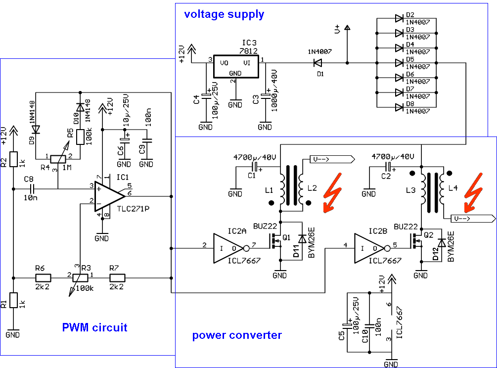
Schematic of the 3rd generation spark inductor with PWM and double MOSFET drive.
(click on the image to view it in full size)
The circuit of the spark inductor consists of 3 parts
1. voltage supply and regulator
2. PWM circuit
3. pulse former and primary coil drive
I'm going to describe each of the parts in more detail now.
1. The voltage supply
The apparatus is getting its power from an external DC power supply with a voltage of 12-30V and
a current capability of up to 5A. Most of the power is consumed by the two ignition coils. To separate
the ESD sensitive CMOS PWM circuitry from spikes on the power supply which killed an OP already during some
test runs, the supply of the coils and the CMOS part is each coupled through diodes to the common positive supply.
Further on the CMOS part is supplyed through a 12 linear regulator circuit to make it independent from the
actual external voltage. The 7812 can be replaced by a 7815 to get 15V in the CMOS part instead which
would slightly increase the slew rate of the MOSFET gate driver ICL7667.
2. The PWM circuitry
The PWM circuit uses a CMOS operational amplifier to build up an RC oscillator with adjustable charge/discharge of
the timing capacitor: This results in a variable frequency, variable duty cycle output signal to the
power MOSFET gate drivers. With the given values the frequency goes from some few discharges per
second up to some kHz with a duty cycle roughly between 10% and 90%. The discharge rate can be changed
further by replacing the timing capacitor C8 of 10nF to a larger one for lower or a smaller one for higher frequencies.
The operational amplifier has to go rail-to-rail with its output signal, otherwise the lower threshold
of the gate driver ICL7667 (1.3V) is not met and thus the MOSFET never turns on.
3. The "power" part
The gates of the two power MOSFETs BUZ22 (Vds=100V - avalanche rated, Id=34A, Ron=0.055Ohm) are
controlled by a special driver circuit ICL7667 from Intersil/Harris. This is an 8pin DIP chip, containing two
CMOS inverters designed to drive large capacitive loads like power MOSFET gates. It would work to
control the gates directly by a standard CMOS output or a CMOS driver like the 4049, but in order
achieve a high slew rate on the gate, a large current is needed to charge/discharge the gate
capacity. The two primary coils of the ignition coils are driven between the positive supply and ground
through drain-source of the power MOSFETs. I mounted the MOSFETs on small heatsinks, but the
power dissipation is so low in the MOSFETs that they are staying cool anyway.
!!! WARNING !!!
The drain of the MOSFETs is connected to the metal tab of the TO-220 package. As
you can see from the oscillograms below, the drain voltage under operation is much higher than the operating voltage
(up to and even above the rated avalanche voltage of the MOSFETs, Uds >120V in my setup). If mounted on
heat sinks, the MOSFETs should be mounted with an isolation set. NEVER touch the MOSFET package under operation!!!
The coils themselves are connected antiparallel to the
supply voltage, thus giving a differential output voltage of twice the single output. Parallel to the internal drain-source
freewheeling diode of the MOSFETs I coupled a set of fast switching diodes BYM26E. The two 4700µF capacitors should be mounted
close to the coil connection, the freewheeling diodes close to the transistor S/D contacts. The connection between
the coil and the driving MOSFET should be made with sufficently thick wire (1mm2or more). I had
a significant voltage drop on a 7x0.52mm cable which I could drastically reduce by going to a 27x0.25mm
both having the same area of 1.5mm2.
| Partlist | ||||
|---|---|---|---|---|
| C1 | 4700µF/40V | |||
| C2 | 4700µF/40V | |||
| C3 | 1000µ/40V | |||
| C4 | 100µ/25V | |||
| C5 | 100µ/25V | |||
| C6 | 10µ/25V | |||
| C8 | 10n | timing capacitor, can be changed from 100pF-10µF | ||
| C9 | 100n | |||
| C10 | 100n | |||
| D1 | 1N4007 | diodes D1-D7 can be replaced by a single, larger diode | ||
| D2 | 1N4007 | |||
| D3 | 1N4007 | |||
| D4 | 1N4007 | |||
| D5 | 1N4007 | |||
| D6 | 1N4007 | |||
| D7 | 1N4007 | |||
| D8 | 1N4007 | |||
| D9 | 1N4148 | |||
| D10 | 1N4148 | |||
| D11 | BYM26E | fast, soft-recovery, 1000V, 2.03A (19A pulse) | ||
| D12 | BYM26E | fast, soft-recovery, 1000V, 2.03A (19A pulse) | ||
| IC1 | TLC271P | LinCMOS OP, single supply | ||
| IC2 | ICL7667 | CMOS dual inverting power MOSFET driver | ||
| IC3 | 7812 | |||
| Q1 | BUZ22 | Vds=100V - avalanche rated, Id=34A, Ron=0.055Ohm | ||
| Q2 | BUZ22 | Vds=100V - avalanche rated, Id=34A, Ron=0.055Ohm | ||
| R1 | 1k | |||
| R2 | 1k | |||
| R3 | 100k, lin | |||
| R4 | 1M, lin | |||
| R5 | 100k | |||
| R6 | 2k2 | |||
| R7 | 2k2 | |||
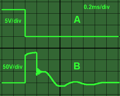
Oscilloscope image of the power MOSFET gate voltage (A) and the power MOSFET drain voltage (B) under operation.
(click on the image to view it in full size)
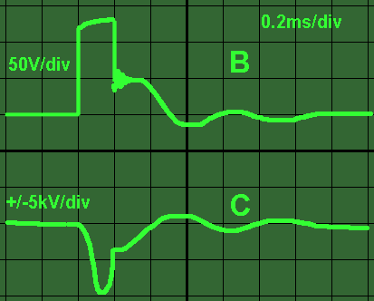
Oscilloscope image of the power MOSFET drain voltage (B) and the high voltage on the open contact of the secondary coil. The polarity of the HV signal
depends on the current direction through the primary coil.
(click on the image to view it in full size)
- soon to come -
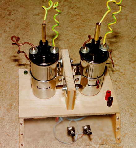
The spark inductor just before a first test run. The two variable resistors of the PWM circuit are on the front plate to allow for adjustments.
(click on the image to view it in full size)
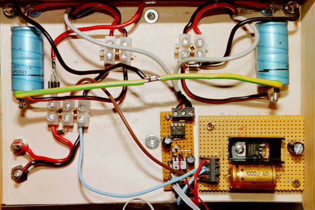
Underneath the spark inductor: the electronics. The 12V regulated power supply for the
oscillator and the oscillator itself are mounted on two pieces of circuit board. The blocking capacitors are mounted separately, as are the protection
and freewheeling diodes. The power MOSFETs are mounted on the upper side behind the coils on small heat sinks.
(click on the image to view it in full size)
Responsible for these pages: U. Zimmermann