The abbreviation CMOS stands for complementary MOS. This technology integrates both n-channel and p-channel MOSFETs on the same chip, resulting in extremely low-power devices with wide ranges of supply voltage.
1. Technology
2. Function
3. Application
The components of integrated CMOS circuits are field effect transistors
of the enhancement MOS type with both, p- and n-channel conductivity.
These transistors are most often formed on a low doped (low conductivity)
n-type silicon substrate. Into this substrate a p-type tub or well is implanted
for n-channel devices and an n-type well or tub for p-channel devices. Into these areas
the source and drain regions are implanted with the opposite conduction type
(i.e. n-type implantation into the p-type well to form an n-channel MOSFET).
The gate contact made of polycrystalline silicon is formed over a thin
isolating oxide layer. drain, gate and source are isolated from each other by thick silicon
dioxide barriers as are different transistors against each other.
CDue to the absence of biasing resistors the CMOS technology is scalable, consumes low power and the transistors
are quite fast. Thus this technology has become the major technology for
verly large scale integrated circuits (VLSI), for example modern microprocessors with
more than 10 million transistors per 1cm x 1cm chip area. The scaling is measured against
the smallest feature size which normally is the length of the gate electrode seen in the
direction from source to drain (see: MOSFET![]() ).
).
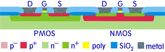
Cross section through a CMOS device showing both n- and p-channel MOSFETs.
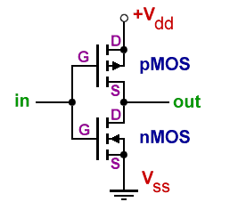
Schematic of a single stage CMOS inverter.
The principle of a CMOS circuit can be seen from its schematic. The threshould voltages of
the n-MOS and p-MOS transistors are chosen to a value that allows for the p-MOS transitors to form their
channel on a gate voltage Vg<0.5Vdd while the channel in the n-MOS transistors
is formed for Vg>0.5Vdd. Thus an inverter consists of just one n-MOSFET and
one p-MOSFET series connected between the positive supply Vdd and the negative supply Vss
with both gates connected to the input.
Because the subthreshould current through a MOSFET is low, there is almost no current
going from the positive to the negative supply as either the p-MOSFETs or the
n-MOSFETs are in the non-conducting state. This is the reason for the low static power consumption of CMOS
ciruits. However during transients, the charge on the gate electrodes has to be moved and for a very narrow voltage
interval of the changing input signal, both transistors can actually become conductive. This
leads to an almost linear increase of power consumption with switching frequency for CMOS devices.
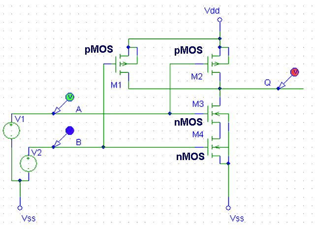
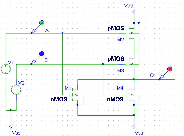
Schematic of a 2 input CMOS NAND gate (left hand side) and NOR gate (right hand side).
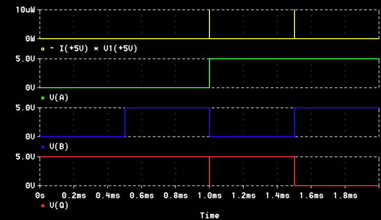

Logic response and power consumption of a 2 input CMOS NAND gate (left hand side) and NOR gate (right hand side). (pspice simulation)
Transfer function of a CMOS inverter. The output voltage is ploted as a function of the input voltage. (pspice simulation)
The early CMOS devices of the 40xx family were very sensitive to electrostatic discharges
damaging the thin gate oxide and destroying the chip. Most of today's CMOS devices are protected
against damage by a set of diodes connecting the inputs to the supply voltage rails which in turn
are connected to the drains, sources and the substrate. This first series of CMOS devices had a much wider
supply voltage range than the TTL family but they were also significantly slower especially if used at a +5V supply voltage.
In order to use CMOS and TTL in the same circuit, the CMOS devices usually had a +12V supply, making level
conversion between CMOS and TTL necessary. Even if the same supply voltage is used for both CMOS and TTL chips
a level conversion is advised due to the different definition of the logic levels and the limited drive
capability of standard CMOS output stages.
| family | logic "0" | logic "1" | ||
|---|---|---|---|---|
| TTL | < 0.8V | > 2.0V | ||
| CMOS Vdd=+5V | < 30% Vdd < 1.5V | > 70% Vdd > 3.5V |
| Family | operating voltage | temperature range | power per gate | delay time per gate | logic levels | output current | input current |
|---|---|---|---|---|---|---|---|
| 40xxB | +3 to +15V | -40 to +85°C | DC: 0.001mW 1MHz: 1mW | 40ns | L: <30%Vdd H: >70%Vdd | L: 1mA H: 1mA | L: <1µA H: <1µA |
| 74Cxx | +3 to +15V | -40 to +85°C | DC: 0.01µW 1MHz: 1mW | 80ns | L: <30%Vdd H: >70%Vdd | L: 1mA(5V)/8mA(10V) H: 1mA(5V)/8mA(10V) | L: 0.005µA H: 0.005µA |
| 74HCxx | +2 to +6V | -40 to +85°C | DC: 0.0025µW 1MHz: 0.75mW | 8ns | L: <30%Vdd H: >70%Vdd | L: 25mA H: 25mA | L: <1µA H: <1µA |
| 74HCTxx | +4.5 to +5.5V | -40 to +85°C | DC: 0.0025µW 1MHz: 0.75mW | 8ns | L: <0.8V H: >2V | L: 25mA H: 25mA | L: <1µA H: <1µA |
| 74ACxx | +2 to +6V | -40 to +85°C | DC: 0.0025µW 1MHz: 0.75mW | 4ns | L: <30%Vdd H: >70%Vdd | L: 50mA H: 50mA | L: <1µA H: <1µA |
| 74ACTxx | +4.5 to +5.5V | -40 to +85°C | DC: 0.0025µW 1MHz: 0.75mW | 6ns | L: <0.8V H: >2V | L: 50mA H: 50mA | L: <1µA H: <1µA |
| 74FCTxx | +4.5 to +5.5V | -40 to +85°C | DC: 0.05mW 1MHz: 0.75mW | 1.5ns | L: <0.8V H: >2V | L: 50mA H: 50mA | L: <5µA H: <5µA |
| 74LCXxx | +2.3 to +3.6V | -40 to +85°C | DC: 0.0025µW 1MHz: 0.75mW | <6ns | L: <30%Vdd H: >70%Vdd | L: <25mA H: <25mA | L: <5µA H: <5µA |
| 74LVxx | +1.0 to +5.5V | -40 to +85°C | DC: 0.0025µW 1MHz: 0.75mW | 6ns | L: <30%Vdd H: >70%Vdd | L: 25mA H: 25mA | L: <1µA H: <1µA |
| 74LVXxx | +2.0 to +3.6V | -40 to +85°C | DC: 0.0025µW 1MHz: 0.75mW | <11ns | L: <30%Vdd H: >70%Vdd | L: 25mA H: 25mA | L: <1µA H: <1µA |
Responsible for these pages: U. Zimmermann