The abbreviation TTL stands for transistor-transistor-logic and has been the well known standard for integrated logic circuits for decades. The 74xx series moved on to modern technologies, but still the chips inherit their functionality from the late 1960's TTL devices.
1. Technology
2. Function
3. Application
The basic components of integrated TTL circuits are resistors and
NPN transistors. These structures are formed on typically moderately p-type
doped silicon wafers with an epitaxial n-type doped layer on top.
Before the n-layer is grown, a highly p-type doped surface layer is formed on the
substrate to serve as channel stop. A buried highly n-type layer underneath
each transistor is also formed by ion implantation.
The base area and the current path for resistors is then formed by p-type (boron)
ion implantation overcompensating the n-type doping in the epitaxial layer.
The emitter area is formed by another n-type doping, partly overcompensating
the p-type base implantation.
A schematic cross-section of both, a transistor and a resistor are shown below.
The value of the resistor - typically some hundred ohms to some ten kilo ohms
is determined by the width-to-length ratio of the implanted p-type current path.
All integrated devices on a chip are isolated against each other by silicon dioxide regions.
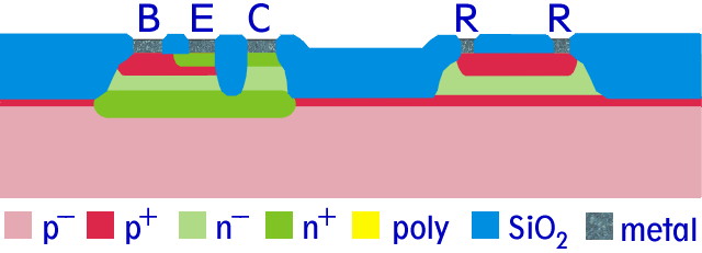
Cross section of the basic parts of an integrated TTL circuit: an NPN transistor and a resistor.
The schematic of a type 7400 2-input NAND gate shows the totem-pole output stage as well as
the emitter coupled inputs. The input transistors are integrated with
a common-base, common-collector, multi-emitter transistor and only drawn here separately
for clearance and simulation purposes.
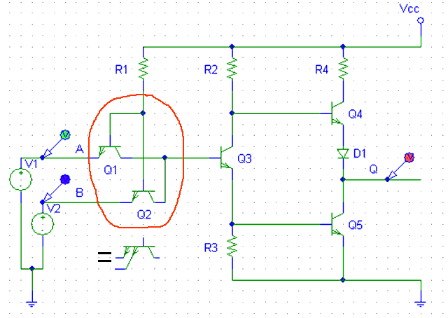
Schematic of a 2 input TTL NAND gate of the 7400 type.
(R1=4k, R2=1.6k, R3=1k, R4=130)
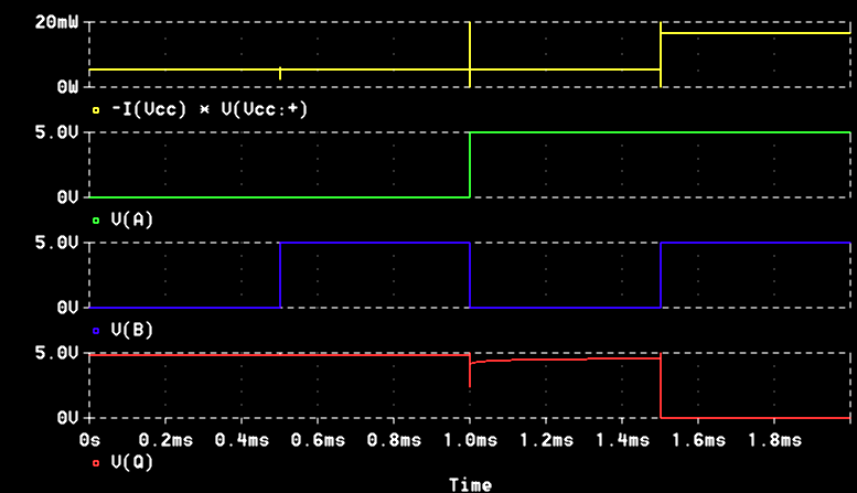
Logic response and power consumption of a 2 input TTL NAND gate. (pspice simulation)
Transfer function of a TTL inverter. The output voltage is ploted as a function of the input voltage. (pspice simulation)
The 74xx series and its 54xx counterpart with militaric specifications (wider operating
temperature and voltage range) defined todays standard for microelectronic devices with
low densities of gates per chip. The highest integrated family members count approximately
a few hundred transistors and as many resistors on one chip. The available functions in the
TTL family range from single gates to counters with on-chip decoders and drivers. TTL chips
are not of wide use anymore because of their comparably poor performance - they are slow and
power consuming. Pin compatible devices were fabricated by almost every manufacturer. They
have been replaced by advanced technologies like
Low-Power Schottky or CMOS.
As of today (march 2000) TTL circuits are still available from
Texas Instruments (www.ti.com)
and Fairchild (www.fairchildsemi.com)
| Family | operating voltage | temperature range | power per gate | delay time per gate | logic levels | output current | input current |
|---|---|---|---|---|---|---|---|
| 74xx | 4.75-5.25V | 0 to 70°C | 10mW | 10ns | L: <0.8V H: >2.0V | L: 16mA H: 0.4mA | L: 1.6mA H: 0.04mA |
| 54xx | 4.5-5.5V | -55 to +125°C | 10mW | 10ns | L: <0.8V H: >2.0V | L: 16mA H: 0.4mA | L: 1.6mA H: 0.04mA |
Responsible for these pages: U. Zimmermann