After the first two parts of this series
where I investigated the possibility of the Atmel ATmega series microcontrollers to select the internal bandgap voltage VBG as input for the analog-to-digital converter. Using the analog supply voltage AVcc as reference for the conversion this allows you to measure the chip’s supply voltage without using any pin or any external devices.
However, when implementing this feature into a project prototype I observed a strange behavior. The datasheet and the big internet were not very helpful in this respect, recommending among other things to discard the first conversion result, but this did not result in concise results either.
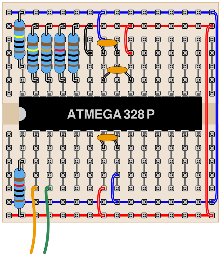
It became obvious that the reason for this behavior was a highly resistive connection between the VBG source and the sample-and-hold capacitor. I went over to a new breadboard and set up a versatile test circuit:
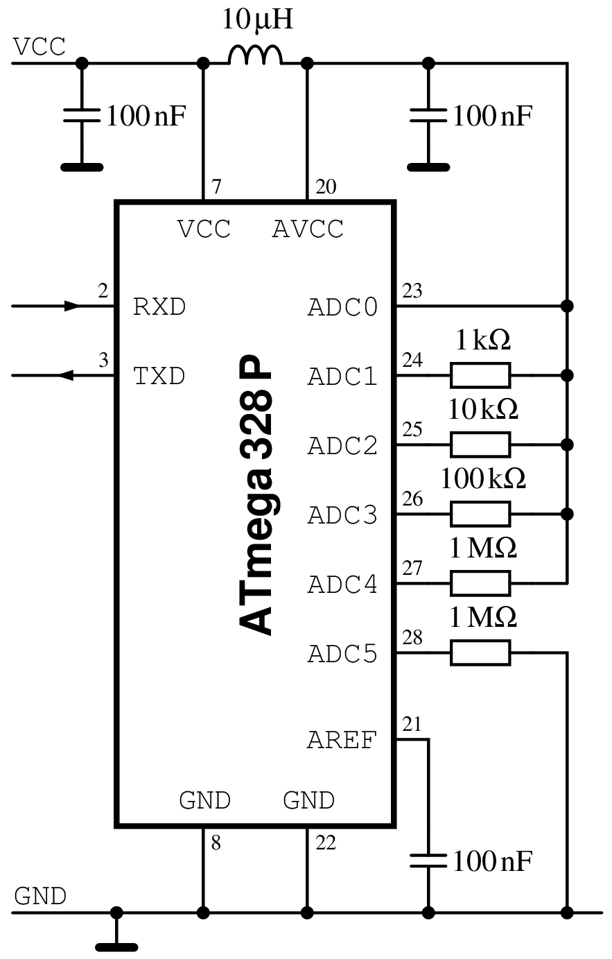
In this test circuit I connected the ADCx inputs of the ATmega328P to the supply rails through differently sized resistors:
- ADC0 directly connected to AVcc
- ADC1
 to AVcc
 - ADC2
 to AVcc
 - ADC3
 to AVcc
 - ADC4
 to AVcc
 - ADC5 to GND
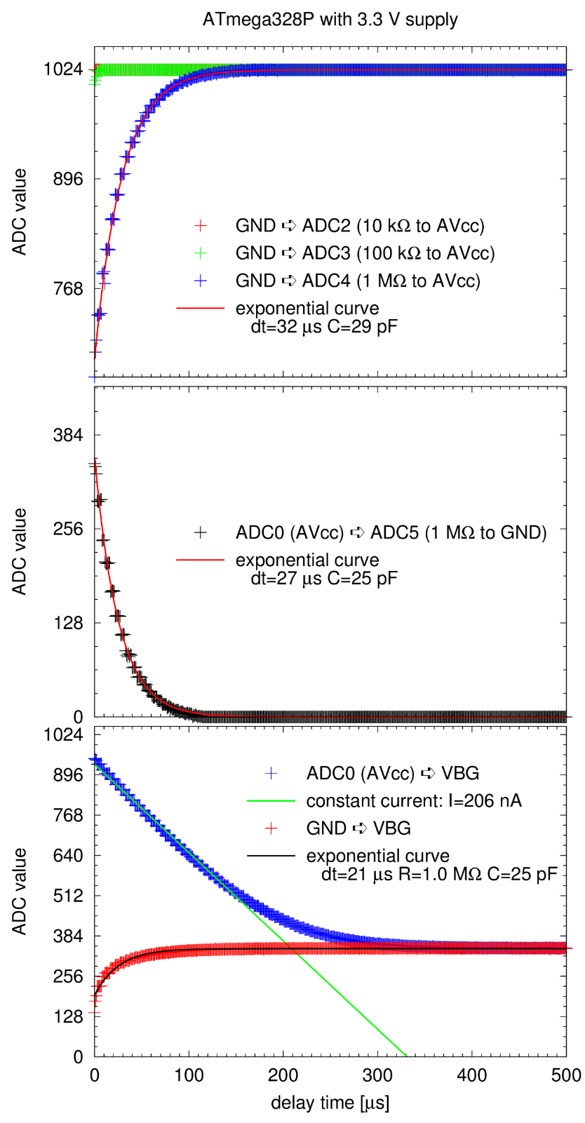
By charging the sample-and-hold capacitor from one channel of the input multiplexer and then switching to another channel it is possible to extract the dynamic properties of the analog-to-digital converter section inside the ATmega.
As can be seen from the graphs below, the sample-and-hold capacitor inside the ATmega328P appears to be about  and thus larger than the value of
  from the datasheet. The datasheet recommends a source impedance of or below – interestingly, the designers at Atmel themselves did not follow this recommendation when they designed the connection of the VBG source to the input multiplexer. The impedance for this connection appears to be in the order of but apart from this the connection is asymmetric with a source which can rather source than sink a current.

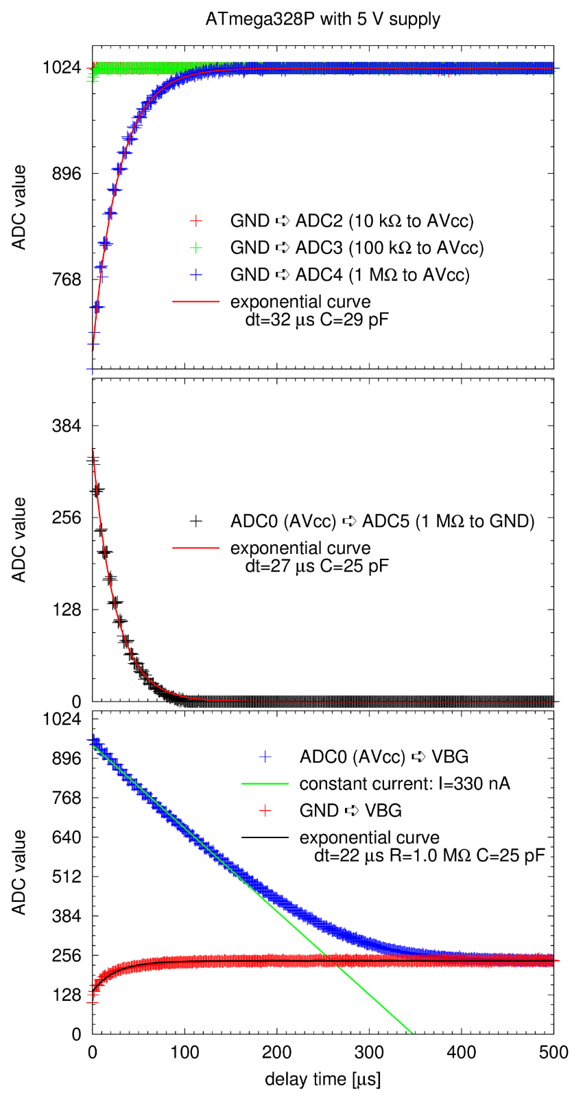
The above data was collected using a  quartz crystal and an assembler loop for the timing delay in steps of
  . The charging of the sample-and-hold capacitor before switching channels was done for
  from a low-resistance conenction to either AVcc (external, ADC0) or GND (internal). The ATmega328P has a datecode of “1312”.

Pingback: ATmega328P – measuring its own supply voltage II « GreenPhotons